

Samsung Ships First 12-Layer HBM4E Memory Samples
Samsung Ships First 12-Layer HBM4E Memory Samples as AI Memory Arms Race Escalates
Hook: Samsung Electronics has begun shipping industry-first 12-layer HBM4E (High Bandwidth Memory 4 Enhanced) samples to major customers, just four months after commencing commercial shipments of HBM4 in February 2026. Unveiled at NVIDIA’s GTC conference in March 2026, HBM4E represents the next leap in memory bandwidth for AI accelerators — delivering over 2 terabytes per second of bandwidth per stack. The move cements Samsung’s position in a memory arms race against SK hynix, with enormous implications for NVIDIA’s next-generation Rubin architecture and for China’s efforts to build a self-sufficient AI supply chain.

Photo by Luka Borazan on Unsplash
What Happened — Samsung’s HBM4E Milestone
Samsung confirmed in early June 2026 that it has begun distributing 12-layer HBM4E engineering samples to key customers, including NVIDIA and other hyperscaler chip designers. The samples feature 12 DRAM dies stacked using through-silicon via (TSV) hybrid bonding technology, paired with an advanced logic base die that handles memory management and error correction. Each stack delivers a bandwidth exceeding 2 TB/s — roughly 66% more than HBM3E and 25% above first-generation HBM4 — while maintaining power efficiency improvements of approximately 20% per bit transferred.
The speed of Samsung’s progression is notable. The company began commercial volume production of HBM4 (8-layer) in February 2026, unveiled the HBM4E architecture at NVIDIA’s GTC in March, and is now shipping 12-layer samples by June. Samsung has indicated it expects HBM4E to enter mass production by Q4 2026, aligning with the ramp of NVIDIA’s Rubin R100 GPU platform, which is scheduled for 2027 deployment.
The 12-layer stack is made possible by Samsung’s proprietary hybrid bonding process, which replaces the conventional micro-bump TSV approach with direct copper-to-copper bonding. This reduces the inter-die gap from approximately 40 microns to under 10 microns, enabling more layers within the same z-height constraint of 3.5mm imposed by GPU package specifications. Samsung is using its 1b-nanometer (fifth-generation 10nm-class) DRAM process for the individual dies, achieving a per-die capacity of 24Gb (3GB), for a total stack capacity of 36GB.
Why It Matters — The Memory Bottleneck in AI Compute
High Bandwidth Memory has become the single most critical bottleneck in AI accelerator performance. Modern large language models require massive parameter counts held in fast-access memory directly adjacent to the compute die. NVIDIA’s H100 used 6 stacks of HBM3 (80GB total); the B200 moved to 8 stacks of HBM3E (192GB); and the Rubin R100 is expected to require HBM4E to reach its targeted 288GB+ memory capacity with sufficient bandwidth to keep its compute cores fed.
The strategic importance of HBM has transformed the competitive dynamics of the memory industry. HBM carries ASPs (average selling prices) roughly 5-6x higher per bit than conventional DDR5 DRAM, making it the highest-margin product in the memory sector. TrendForce estimates the HBM market will reach $38 billion in 2026, up from $24 billion in 2025, with HBM4 and HBM4E driving the next wave of growth. Samsung, SK hynix, and Micron are the only three companies worldwide capable of producing HBM at scale — and Samsung’s 12-layer HBM4E sample shipment signals it is determined to close the gap with SK hynix, which has historically led in HBM market share.
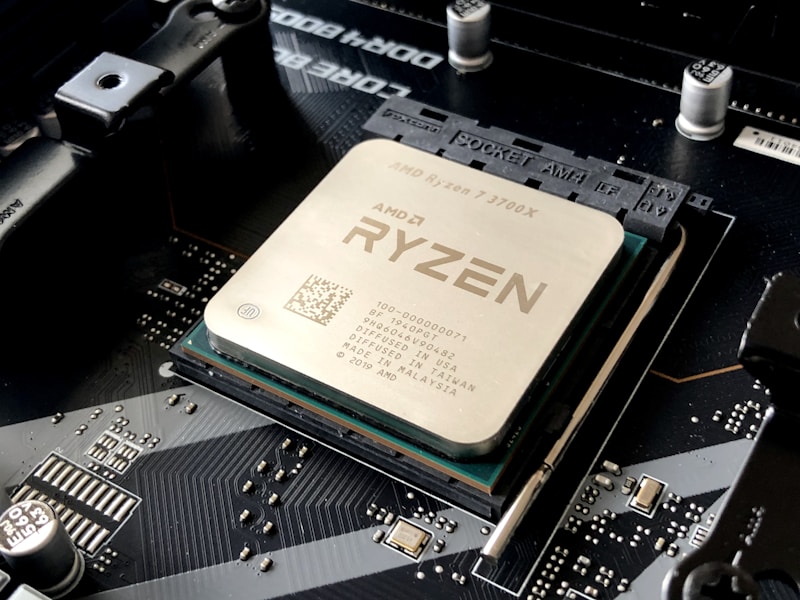
Photo by Brett Jordan on Unsplash
Key Data — The Evolution of High Bandwidth Memory
| Generation | Year | Max Layers | Bandwidth/Stack | Capacity/Stack | Interface Width | Key Adopter |
|---|---|---|---|---|---|---|
| HBM | 2015 | 4 | 128 GB/s | 4 GB | 1024-bit | AMD Fiji GPU |
| HBM2 | 2016 | 8 | 256 GB/s | 8 GB | 1024-bit | NVIDIA P100 |
| HBM2E | 2020 | 8 | 460 GB/s | 16 GB | 1024-bit | NVIDIA A100 |
| HBM3 | 2022 | 12 | 819 GB/s | 24 GB | 1024-bit | NVIDIA H100 |
| HBM3E | 2024 | 12 | 1.2 TB/s | 36 GB | 1024-bit | NVIDIA H200 / B200 |
| HBM4 | 2026 | 8 (12 planned) | 1.6 TB/s | 32 GB | 2048-bit | NVIDIA Rubin (expected) |
| HBM4E | 2026-27 | 12 | 2.0+ TB/s | 36 GB | 2048-bit | NVIDIA Rubin R100 (expected) |
Sources: Samsung, SK hynix, JEDEC specifications, NVIDIA product announcements, TrendForce. HBM4E specs based on Samsung’s announced sample specifications; final production specs may differ.
Strategic Implications — Samsung vs. SK hynix and the China Factor
Samsung’s HBM4E push is as much about competitive positioning as it is about technology leadership. SK hynix has dominated the HBM market since its inception, capturing an estimated 50-53% market share through 2025, compared to Samsung’s 35-38% and Micron’s 10-12%. SK hynix was also first to market with HBM3E in volume, securing the lion’s share of NVIDIA’s B200 orders. Samsung’s early 12-layer HBM4E samples represent an attempt to leapfrog SK hynix and establish first-mover advantage in the next-generation memory tier.
The implications for China’s semiconductor ecosystem are significant. Chinese AI chipmakers — including Huawei, Cambricon, Hygon, Moore Threads, and Enflame — are designing next-generation accelerators that will require HBM-class memory. However, under current U.S. export controls, advanced HBM shipments to China are restricted. SK hynix and Samsung have both received temporary licenses for certain legacy HBM products, but HBM4 and HBM4E fall squarely within restricted categories. This creates a critical supply gap for Chinese AI chip designers who need cutting-edge memory to compete with NVIDIA’s performance benchmarks.
China’s domestic DRAM champion, CXMT (长鑫存储), is capable of producing DDR5 and LPDDR5 but has not yet demonstrated HBM production capability. Building an indigenous HBM supply chain would require not only advanced DRAM process technology but also TSV hybrid bonding equipment — much of which is controlled by Japanese and European equipment makers subject to allied export restrictions. The timeline for a viable Chinese HBM alternative remains at least 3-5 years, leaving Chinese AI chipmakers dependent on stockpiled inventory and workarounds in the interim.
Market Signal — What to Watch Next
NVIDIA’s Rubin memory configuration: NVIDIA’s next-generation Rubin GPU platform, expected to tape out in late 2026 and ship in 2027, will be the primary demand driver for HBM4E. The number of HBM4E stacks per GPU (8 vs. 12) and the total memory capacity will determine the volume requirements for both Samsung and SK hynix. Any indication that NVIDIA is dual-sourcing HBM4E from both vendors would validate Samsung’s technology readiness.
SK hynix’s response: SK hynix is expected to begin its own 12-layer HBM4E sampling by Q3 2026. The speed and yield of Samsung’s production ramp relative to SK hynix will determine whether the market share balance shifts in 2027. SK hynix’s advantage in advanced packaging (it has been shipping 12-layer HBM3E in volume since 2025) gives it an incumbency edge, but Samsung’s hybrid bonding technology could prove disruptive if yields are competitive.
China’s HBM workaround strategies: Watch for developments in three areas: (1) CXMT’s HBM R&D announcements, which would signal Beijing’s intent to build an indigenous memory stack; (2) Chinese companies stockpiling HBM3E inventory before further export restrictions take effect; and (3) alternative memory architectures such as CXL-attached memory or LPDDR5X-based chiplet designs that could partially substitute for HBM in constrained environments.
The outcome will shape not only the competitive dynamics of the $38 billion HBM market but also the trajectory of US-China technology decoupling, where memory has emerged as one of the most consequential chokepoints.
CII Analysis
Samsung’s 12-layer HBM4E sample shipment is a technically significant milestone that underscores the accelerating pace of memory innovation driven by AI demand. The transition from HBM3E to HBM4E in barely two years represents the fastest generational cadence in HBM history, reflecting the urgency with which both memory makers and GPU designers are racing to solve the memory wall problem in AI computing.
From China’s perspective, the HBM4E announcement highlights an uncomfortable reality: the memory bottleneck is tightening precisely when Chinese AI chipmakers need it to ease. The gap between what CXMT can produce (conventional DDR5/LPDDR5) and what NVIDIA’s next-generation accelerators require (12-layer HBM4E with 2+ TB/s bandwidth) is widening, not narrowing. This asymmetry will increasingly shape Chinese AI chip design strategies, pushing domestic designers toward architectures that can tolerate lower memory bandwidth — or toward creative packaging solutions that circumvent the HBM dependency entirely.
Our assessment: HBM has become the most strategically consequential component in the AI hardware stack after the GPU die itself. Samsung’s early 12-layer HBM4E samples signal that the competitive gap with SK hynix is narrowing, which is positive for GPU makers seeking supply diversification. For China, however, the advancement underscores the depth of the memory technology gap and the long timeline required to build an indigenous HBM supply chain. The companies and governments that control HBM production will have outsized leverage over the global AI infrastructure buildout for the remainder of this decade.
For more analysis on China’s semiconductor ecosystem, see our China Semiconductor Ecosystem pillar page and our coverage of US-China semiconductor decoupling.
Further Reading:
- CXMT IPO Creates Windfall for China Chip Supply Chain
- Tencent-Backed Enflame IPO as China AI Chip Wave Rises
- China Opens First Photonic Computing Lab to Sidestep US Chip Curbs
Sources
- Samsung Newsroom — Samsung Begins Shipping 12-Layer HBM4E Samples (June 2026)
- Samsung Semiconductor — HBM Product Page
- NVIDIA — GTC March 2026 Announcements
- TrendForce — HBM Market Forecast and Supply Chain Analysis (2026)
- AnandTech — Samsung HBM4E: Architecture Deep Dive (March 2026)
- JEDEC — JESD270 HBM4 Specification