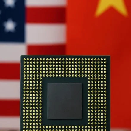

Huawei Proposes New Chip Path as China Semiconductor Self-Reliance Drive Intensifies
Huawei proposes a novel chiplet design methodology as China accelerates semiconductor self-sufficiency. SMIC and HLMC expand mature-node capacity while the EUV gap persists.
Huawei’s Chip Design Breakthrough Signals New Direction
Huawei Technologies has proposed a fundamentally new approach to chip architecture that could reshape China’s semiconductor trajectory, according to a Reuters report published on June 19, 2026. The proposal, outlined in a technical white paper distributed to Chinese foundry partners and research institutes, describes a “composable chiplet” methodology that allows multiple smaller dies manufactured on different process nodes to function as a unified processor — sidestepping the need for cutting-edge EUV lithography that remains restricted under US export controls.
The approach leverages advanced packaging techniques to interconnect chiplets fabricated on SMIC’s 7nm (N+2) process with those on more mature 28nm and 14nm nodes, creating heterogeneous processors that Huawei claims achieve 70-85% of the performance of monolithic chips built on TSMC’s 5nm process. The white paper positions this as a “scalable path to sustained compute growth without access to sub-7nm fabrication.”
The proposal arrives at a critical juncture. China’s semiconductor imports fell to $349 billion in 2025, down from a peak of $415 billion in 2021, as domestic substitution accelerated across automotive, industrial, and consumer electronics sectors. The Chinese government’s target of 70% chip self-sufficiency by 2025 was not met — industry estimates place actual self-sufficiency at roughly 23% for advanced logic — but the trajectory is unmistakably upward.
SMIC and HLMC Accelerate Mature-Node Expansion

Semiconductor Manufacturing International Corporation (SMIC), China’s largest contract chipmaker, reported Q1 2026 revenue of $1.89 billion, up 21% year-over-year, driven by surging demand for its 28nm and 14nm nodes. The company’s monthly capacity reached 850,000 200mm-equivalent wafers in Q1 2026, up from 720,000 a year earlier. SMIC’s capital expenditure for 2026 is budgeted at approximately $9.5 billion, with the bulk directed toward expanding mature-node capacity at its Shanghai, Beijing, and Shenzhen fabs.
Hua Hong Semiconductor (HLMC), China’s second-largest foundry, posted Q1 2026 revenue of $680 million, with its Wuxi 12-inch fab reaching 95% utilization — up from 82% in Q4 2025. HLMC specializes in specialty processes including BCD (bipolar-CMOS-DMOS) for power management, embedded non-volatile memory, and CIS (CMOS image sensor) platforms. The company’s 55nm and 90nm BCD platforms are particularly critical for China’s EV supply chain, where domestic content requirements are tightening.
Together, SMIC and HLMC now account for approximately 8.5% of global foundry revenue, according to TrendForce’s Q1 2026 rankings — up from 6.2% in Q1 2023. While this pales in comparison to TSMC’s dominant 62% share, the growth rate signals that Chinese foundries are capturing an increasing share of the non-bleeding-edge market.
The Process Gap: China vs. TSMC and Samsung

| Capability | TSMC | Samsung | SMIC | HLMC |
|---|---|---|---|---|
| Most Advanced Node (Logic) | 2nm (N2) risk production | 3nm GAA (SF3) | 7nm (N+2, limited) | 28nm (bulk) |
| EUV Lithography | Yes (ASML NXE:3800E) | Yes (ASML NXE:3600D) | No (sanctioned) | No |
| Advanced Packaging | CoWoS, InFO, SoIC | I-Cube, X-Cube | 2.5D interposer (emerging) | Fan-out WLP |
| 2026 Capex (Est.) | $32-36B | $15-18B | $9-10B | $2-3B |
| Global Foundry Share | 62% | 11% | 5.5% | 3.0% |
| Primary Customers | Apple, NVIDIA, AMD, Qualcomm | Samsung LSI, Qualcomm, Google | Huawei HiSilicon, UNISOC, domestic IoT | Automotive Tier-1, IoT, power ICs |
The EUV gap remains the single largest structural disadvantage. ASML’s Twinscan NXE scanners, which use 13.5nm wavelength extreme ultraviolet light, are required for high-volume manufacturing at 5nm and below. The Netherlands, under pressure from Washington, has not granted export licenses for EUV tools to Chinese customers since 2019. China’s domestic lithography effort, led by Shanghai Micro Electronics Equipment (SMEE), has demonstrated a 28nm-capable DUV immersion scanner but remains years away from EUV-equivalent technology.
TSMC’s 2nm (N2) node entered risk production at its Hsinchu fab in late 2025, with volume production expected in H2 2026. The node uses gate-all-around (GAA) nanosheet transistors — a fundamental departure from FinFET — delivering 15% higher performance or 30% lower power versus 3nm at the same transistor density. Samsung’s 3nm GAA (SF3) process is already in volume production, with 2nm (SF2) expected in 2027.
SMIC’s most advanced production node remains its 7nm (N+2) process, achieved through multi-patterning on DUV immersion tools — a technically impressive feat that comes with significant yield and cost penalties. Industry analysts estimate SMIC’s 7nm yield at 50-60%, compared to TSMC’s 90%+ for comparable nodes, and the cost per good die is estimated at 3-4x that of TSMC’s 7nm. Huawei’s Hisilicon division has used SMIC’s 7nm for its Kirin 9000S and Kirin 9010 smartphone processors, but volumes remain constrained.
Equipment Localization: The Quiet Revolution
Beyond foundries, China’s semiconductor equipment sector is undergoing rapid transformation. Naura Technology (NAURA), China’s largest domestic equipment maker, reported 2025 revenue of 32 billion yuan ($4.4 billion), up 48% year-over-year. Advanced Micro-Fabrication Equipment Inc. China (AMEC) shipped its 500th dielectric etcher in Q1 2026, with its 5nm-capable CCP etcher qualified at multiple domestic logic fabs. ACM Research posted 40% revenue growth in 2025 on the back of its single-wafer cleaning tools.
According to SEMI’s Q1 2026 report, Chinese chip equipment spending is projected to reach $45 billion in 2026, representing roughly 35% of global semiconductor equipment expenditure. The localization rate — the share of equipment purchased from domestic suppliers — has risen from approximately 10% in 2020 to an estimated 25% in 2026, with the Chinese government targeting 40% by 2028 under its “Made in China 2025” successor policy.
The equipment push is critical because it addresses the most acute vulnerability. While US export controls restrict China’s access to advanced chips and manufacturing tools, the domestic equipment buildout creates a parallel ecosystem that can sustain chip production even without Western tools — albeit at lower technology nodes.
Geopolitical Dimensions and the Path Forward
Huawei’s chiplet proposal sits within a broader geopolitical context. The Biden administration’s October 2023 export controls, tightened further in 2024 and 2025, effectively blocked China’s access to advanced AI chips (NVIDIA A100/H100/B100 and equivalents) and restricted sales of semiconductor manufacturing equipment capable of producing chips below 14nm. The Trump administration’s Section 301 tariffs added a 50% duty on Chinese semiconductors — though most Chinese chips flow to domestic consumption rather than US markets.
China’s response has been multi-pronged: massive state investment (the “Big Fund” Phase III at $48 billion), accelerated equipment localization, and architectural innovation — of which Huawei’s chiplet approach is the most visible example. The question is whether these measures, collectively, can narrow the technology gap faster than it widens.
Industry analysts are divided. “China will likely achieve self-sufficiency in 28nm and above within 3-5 years,” said Dan Hutcheson, vice chair of TechInsights, at a May 2026 semiconductor forum. “Below 7nm, the timeline extends to a decade or more, barring a domestic EUV breakthrough.” Others note that China’s sheer scale of investment — approximately $142 billion in total semiconductor subsidies and tax incentives since 2020 — creates momentum that cannot be dismissed.
For global chip buyers, the implication is straightforward: expect growing supply of Chinese mature-node chips at competitive prices over the next 2-3 years, while advanced-node supply remains concentrated in Taiwan and South Korea for the foreseeable future.
Sources
- Reuters, “Huawei proposes new path for chip development as China semiconductor self-reliance drive intensifies,” June 19, 2026 — reuters.com
- TrendForce, Global Foundry Revenue Rankings Q1 2026, June 2026
- SEMI, World Fab Forecast and Equipment Market Report, Q1 2026
- SMIC Q1 2026 Earnings Release, May 12, 2026
- Huawei Technologies, “Composable Chiplet Architecture for Heterogeneous Integration,” Technical White Paper, June 2026
- TechInsights, “China Semiconductor Self-Sufficiency Assessment,” May 2026
- NAURA Technology Group, 2025 Annual Report, March 2026